Double sided printed circuit boards (PCBs) have become an integral component in the world of modern electronics. These versatile boards play a crucial role in powering countless devices we use daily, from smartphones to industrial machinery. By utilizing both sides of the board for component placement and routing, double sided PCBs offer a balance of complexity and cost-effectiveness that makes them ideal for a wide range of applications.
As technology continues to advance, the demand for more compact and powerful electronic devices grows. Double sided PCBs rise to meet this challenge by providing increased design flexibility and improved signal integrity compared to their single-sided counterparts. This enhanced capability allows engineers to create more sophisticated circuits while maintaining a relatively simple manufacturing process. For more detailed information on double sided PCB manufacturing and design considerations, visit icape-group.com , a leading resource in the PCB industry.
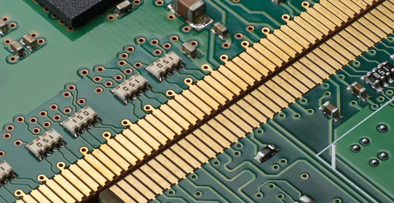
Anatomy and fabrication of double sided PCBs
Double sided PCBs consist of a core substrate material, typically FR-4 fiberglass, with copper layers on both sides. The fabrication process begins with the creation of the circuit design using specialized CAD software. This design is then transferred to the copper layers through a photolithographic process, followed by etching to remove unwanted copper and create the desired circuit patterns.
One of the key advantages of double sided PCBs is their ability to accommodate more complex circuits within a smaller footprint. This is achieved through the use of vias, which are small holes drilled through the board and plated with copper to create electrical connections between the top and bottom layers. The strategic placement of these vias allows for more efficient routing of signals and power throughout the board.
The fabrication process also includes the application of solder mask and silkscreen layers. The solder mask protects the copper traces from oxidation and prevents solder bridges during component assembly. The silkscreen layer, typically white, provides important information such as component designators and polarity markings, facilitating assembly and maintenance.
Copper layer configurations in double sided PCBs
The copper layers in double sided PCBs play a critical role in determining the board’s electrical performance and current-carrying capacity. Different copper thicknesses and configurations are available to meet the diverse requirements of various electronic applications.
Standard 1oz and 2oz copper thickness options
The most common copper thicknesses used in double sided PCBs are 1 oz (35 μm) and 2 oz (70 μm) per square foot. These standard options provide a good balance between conductivity and cost for most applications. The 1 oz copper thickness is suitable for general-purpose designs, while 2 oz copper offers improved current-carrying capacity and heat dissipation for more demanding circuits.
When selecting copper thickness, engineers must consider factors such as current requirements, trace width limitations, and thermal management needs. For example, a 1 oz copper layer might be sufficient for a low-power digital circuit, while a 2 oz layer would be more appropriate for a power supply board handling higher currents.
High-current applications with 3oz+ copper layers
For applications requiring exceptional current-carrying capacity or improved heat dissipation, copper thicknesses of 3 oz (105 μm) or greater can be employed. These thicker copper layers are particularly useful in high-power electronics, automotive applications, and industrial control systems where reliability under extreme conditions is paramount.
It’s important to note that increasing copper thickness also impacts the manufacturing process and overall board thickness. Designers must carefully balance the benefits of thicker copper against potential challenges in etching, drilling, and maintaining tight tolerances.
Copper pour techniques for improved signal integrity
Copper pour techniques involve filling large areas of the PCB with copper, often connected to ground or power planes. This approach offers several benefits, including improved signal integrity, reduced electromagnetic interference (EMI), and enhanced thermal management. By providing a low-impedance return path for signals, copper pours help minimize noise and maintain signal quality.
When implementing copper pours, designers must consider the impact on impedance control and potential issues with thermal stress during manufacturing. Proper use of thermal relief patterns around component pads can help alleviate these concerns while still maintaining the benefits of copper pours.
Via technologies in double sided PCB design
Vias are essential elements in double sided PCB design, enabling connections between the top and bottom layers and facilitating complex routing schemes. Different via technologies offer varying levels of performance and manufacturing complexity.
Through-hole vias for component mounting
Through-hole vias are the most common type used in double sided PCBs. These vias extend from the top layer to the bottom layer and are typically used for mounting components with leads that pass through the board. Through-hole vias offer excellent mechanical strength and reliability, making them ideal for applications subject to vibration or mechanical stress.
While through-hole technology has been largely supplanted by surface mount technology (SMT) for many components, it remains relevant for certain types of connectors, power components, and in applications where robustness is a primary concern.
Blind and buried vias for advanced routing
Although less common in double sided PCBs, blind and buried vias can be employed for advanced routing requirements. Blind vias connect an outer layer to an inner layer without passing through the entire board, while buried vias connect inner layers without being visible on the outer layers.
These specialized via types allow for more efficient use of board space and can improve signal integrity by reducing via stub lengths. However, they also increase manufacturing complexity and cost, making them more commonly used in multilayer PCB designs rather than standard double sided boards.
Microvias and HDI technology in compact designs
For extremely compact and high-density designs, microvia technology can be applied to double sided PCBs. Microvias are very small vias, typically less than 150 μm in diameter, that allow for ultra-fine pitch component mounting and routing. This technology is often associated with High-Density Interconnect (HDI) boards, which push the limits of PCB miniaturization.
While microvias and HDI techniques are more commonly found in multilayer boards, they can be applied to double sided PCBs in specialized applications where maximum component density is required within a two-layer constraint.
Solder mask and silkscreen considerations
The solder mask and silkscreen layers play crucial roles in the functionality and usability of double sided PCBs. Proper application and design of these layers can significantly impact the board’s manufacturability, reliability, and ease of assembly.
Selective solder masking techniques
Selective solder masking involves applying the solder mask layer in specific patterns to control where solder can adhere to the board. This technique is particularly useful in double sided PCB designs where components are mounted on both sides of the board. By carefully defining solder mask openings, designers can ensure proper solder joint formation and prevent solder bridges between closely spaced pads.
Advanced selective solder masking techniques can also be used to create solder dams, which help control solder flow during reflow processes. This is especially important for fine-pitch components where precise control of solder volume is critical for reliable connections.
Silkscreen optimization for component identification
The silkscreen layer provides valuable information for assembly, testing, and maintenance of the PCB. Optimizing the silkscreen design is crucial for ensuring clarity and readability, particularly in densely populated double sided boards. Key considerations include:
- Using appropriate font sizes and styles for legibility
- Avoiding overlap with solder mask openings or copper features
- Providing clear orientation markers for polarized components
- Including board revision information and manufacturer identifiers
In double sided designs, it’s important to consider the placement of silkscreen information on both sides of the board. Careful planning ensures that critical information is visible and not obscured by components on the opposite side.
Signal integrity and EMI mitigation in double sided PCBs
Maintaining signal integrity and minimizing electromagnetic interference (EMI) are critical challenges in double sided PCB design. As circuit speeds increase and components become more densely packed, careful attention to these factors becomes increasingly important.
Ground plane design for reduced electromagnetic interference
Effective ground plane design is crucial for managing EMI in double sided PCBs. A well-designed ground plane provides a low-impedance return path for signals, reducing radiated emissions and improving overall signal integrity. In double sided boards, one layer is often dedicated as a ground plane, with strategic use of vias to maintain continuity.
Designers must consider the impact of ground plane splits or discontinuities, which can create unintended antennas and increase EMI. Techniques such as stitching vias and careful routing of high-speed signals can help mitigate these issues.
Controlled impedance routing strategies
Controlled impedance routing is essential for maintaining signal integrity in high-speed digital circuits. In double sided PCBs, this often involves careful consideration of trace width, spacing, and relationship to the ground plane. Common controlled impedance structures in double sided boards include:
- Microstrip lines (signal trace on outer layer with reference to opposite ground plane)
- Coplanar waveguides (signal trace with adjacent ground traces on the same layer)
- Differential pairs for high-speed serial interfaces
Achieving precise impedance control may require close collaboration with the PCB manufacturer to account for material properties and manufacturing tolerances.
Split plane techniques for Mixed-Signal designs
In mixed-signal designs that incorporate both analog and digital circuits on the same double sided PCB, split plane techniques can be employed to isolate sensitive analog sections from noisy digital areas. This typically involves creating separate analog and digital ground regions, connected at a single point to prevent ground loops.
Careful routing of signals across the split plane boundary and judicious use of bypass capacitors are crucial for maintaining signal integrity in these designs. While split plane techniques are more commonly associated with multilayer boards, they can be adapted for use in double sided PCBs with careful planning.
Thermal management in double sided PCB layouts
Effective thermal management is crucial for ensuring the reliability and performance of electronic devices. Double sided PCBs present unique challenges and opportunities for managing heat dissipation.
Copper spreading for heat dissipation
One of the primary techniques for improving thermal management in double sided PCBs is copper spreading. This involves using large copper areas or planes to distribute heat away from hot components. The increased surface area of these copper regions enhances convective and radiative heat transfer to the surrounding environment.
When implementing copper spreading, designers must balance thermal requirements with other considerations such as signal integrity and manufacturability. Techniques such as hatched ground planes can provide a compromise between thermal performance and flexibility for signal routing.
Thermal via arrays for High-Power components
For components that generate significant heat, such as power regulators or high-performance processors, thermal via arrays can be employed to enhance heat dissipation. These arrays consist of multiple vias placed under or around the component, providing a low-thermal-resistance path to the opposite side of the board.
The effectiveness of thermal via arrays depends on factors such as via size, spacing, and plating thickness. In some cases, these vias may be filled with thermally conductive material to further improve heat transfer. Careful analysis and thermal simulation may be necessary to optimize the design of thermal via arrays for specific applications.
PCB material selection for thermal conductivity
The choice of PCB substrate material can significantly impact the board’s thermal performance. While FR-4 is the most common substrate for double sided PCBs, alternatives with higher thermal conductivity may be considered for applications with demanding thermal requirements.
Materials such as aluminum-based PCBs or ceramic substrates offer superior thermal performance but come with trade-offs in terms of cost and manufacturability. For many applications, a balance can be struck by using standard FR-4 materials with optimized copper distribution and careful thermal management techniques.
As the complexity of electronic devices continues to increase, the role of double sided PCBs in modern electronics remains crucial. These versatile boards offer a balance of performance, cost-effectiveness, and design flexibility that makes them indispensable in a wide range of applications. By leveraging advanced fabrication techniques, optimizing copper layer configurations, and employing sophisticated via technologies, designers can push the boundaries of what’s possible with double sided PCBs.
The considerations discussed in this article, from signal integrity and EMI mitigation to thermal management, highlight the multifaceted nature of double sided PCB design. As technology evolves, so too will the techniques and methodologies used to create these essential components of our electronic world. By staying informed about the latest developments and best practices in PCB design, engineers and designers can continue to innovate and create the next generation of electronic devices that will shape our future.